Thermal imaging cameras, pivotal in modern security monitoring, comprise several key thermal imaging components that enhance functionality.
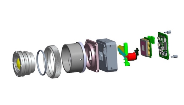
1. Lens and Optics
The lens in a thermal imaging camera can focus infrared energy onto the sensor. The design and material of the lens determine the Field of View (FOV) and the extent of the scene captured by the camera. Taking into account factors such as lens diameter, focal length, and mounting threads, lens assemblies of imaging devices must be customed to fit specific lens sizes and shapes.
Mill-turn machining is the main manufacturing method for imaging device components, ensuring not only accuracy but also proper alignment within the imaging device. The customization of lens housing underscores the significance of each component in manufacturing thermal imaging devices.
2. The Detector
The infrared detector is the main component of infrared thermal imagers and is mainly responsible for capturing infrared energy. The detector’s resolution, defined by its pixel configuration, directly impacts the detail and accuracy of the thermal image.
Additionally, the detector’s thermal sensitivity or Noise Equivalent Temperature Difference (NETD) is a vital specification, reflecting the camera’s ability to discern minute temperature differences. This configuration enables the detection of minute temperature differences, as subtle as 0.01°C, displayed using various color palettes.
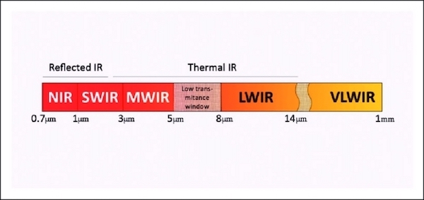
The spectral range is another critical aspect, with most thermal cameras operating in the longwave spectral range of 8µm to 14µm, suitable for various applications from electrical inspections to firefighting.
3. Image Processing and Analysis
The final component is the processing and analysis of the captured infrared data. Advanced thermal imaging devices incorporate image non-uniformity correction, noise removal, and pseudo-color enhancement technologies. These processing techniques refine the raw thermal data, enhancing image quality and readability.
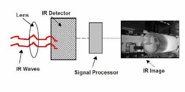
Sophisticated algorithms are employed to interpret the thermal data, enabling the camera to differentiate between objects and backgrounds and to detect anomalies or specific heat signatures. Thermal cameras, leveraging this principle, can function in complete darkness or smoke-filled environments, as they rely on heat signatures rather than visible light. This processed data is pivotal for making informed decisions in security monitoring and other applications.
Designing thermal imaging devices demands meticulous attention to material selection, surface finish, and machined parts assembly. This section delves into these aspects, emphasizing the technicalities and precision necessary for optimal performance.
Material Choice for Thermal Imaging Devices Manufacturing
When manufacturing thermal imaging devices, materials for the housings and components should focus on durability, lightweight construction, and impact resistance.
- Aluminum: Used extensively in imaging devices machining for its lightweight nature, excellent heat dissipation properties, and durability. Aluminum is ideal for Imaging components machining, which can minimize weight while maintaining thermal stability.
- Magnesium Alloy: Chosen for machined parts for imaging components due to its high strength-to-weight ratio. Magnesium alloys boast excellent thermal conductivity and mechanical properties, aligning with the requirements of custom imaging devices.
- Engineering Plastics and Polymers: High-quality polymers are used for their lightweight construction, good thermal insulation, and resistance to impact, chemicals, and environmental conditions. These materials provide additional durability and protection against external impacts, ensuring the longevity and reliability of the device.
- Titanium Alloy:Titanium alloys are valued for their exceptional strength, corrosion resistance, and lightweight properties. They are ideal for applications that demand both durability and minimal weight, contributing to the overall robustness of the imaging devices.
EDM and 5-axis machining are employed to meet tight dimensional specifications of manufacturing imaging devices. Techniques such as laser marking and cutting are always utilized for intricate design requirements and precise manufacturing.
Material selection plays an important role when custom imaging devices. Coupled with advanced machining techniques, these materials are transformed into components that enhance the functionality and durability of thermal imaging devices.
Surface Finish for Machined Imaging Components
In imaging devices machining, high-quality as-machined finish allows for optimal performance of the device such as lens mounts or structural housings.
Anodizing or chemical film coatings can not only improve corrosion resistance but also enhance thermal emissivity, vital for components exposed to infrared radiation in imaging devices.
Hard oxidizing enhances the aluminum’s surface hardness and wear resistance, making it suitable for rugged environments. This process also improves the material’s corrosion resistance and thermal insulation properties, which are crucial for the stability and longevity of thermal imaging devices.
In military applications, the durability of these components may be further augmented by military-grade spray paint, ensuring resilience under extreme conditions.
Any misalignment or defect in the assembly could hinder their accuracy and sensitivity.
One critical aspect of assembly testing is ensuring the sealing and fit performance of the components. Proper sealing is essential for IP67 protection. The IP67 rating signifies that the device is fully protected against dust ingress and can withstand temporary immersion in water, making it suitable for various challenging environmental conditions.
Vibration resistance and shock absorption testing ensure sensor reliability in environments with high vibrations and potential shocks.
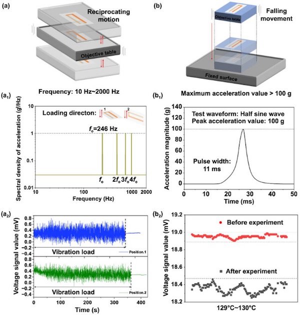
The diagrams and graphs provided in this Fig illustrate tests conducted on flexible temperature sensors to assess their shock and vibration resistance. The vibration test subjected the sensor to frequencies from 10 Hz to 2000 Hz and monitored the output under different conditions. The shock test evaluated the sensor’s ability to withstand a 100 g force, simulating a sudden impact. The results, including real-time sensor output and temperature stability (129 °C–130 °C), indicated the sensor’s robustness against mechanical stresses.
Finally, thermal imaging devices are often subjected to various environmental tests including exposure to varying temperatures, humidity, and other environmental factors, to ensure they can operate effectively under different conditions.
The multi-sensor enhanced driver vision system is a multi-band imaging system that can be mounted on land, sea and air vehicles, and enable more efficient and frequent site and equipment inspections for large-scale critical infrastructure and heavy industrial sites. It typically combines digital sensors to provide appropriate situational awareness in darkness, smoke, smog, fog, and other atmospheric obscurants normally invisible to the naked eye. Mounted on industrial drones, this multi-sensor imaging device allows close-up visual and thermal observations and minimizes safety and operational risks.
This multi-sensor imaging device consists mainly of a sensing system, a data analysis system, a main metal frame, and an outer shell. The sensing system detects and collects characteristic signals from the external environment through sensor components with different characteristics. The data analysis system is responsible for combining, analyzing, and outputting the information collected by the sensing system. The metal frame plays a role in fixing and protecting the components of the sensing system and the data analysis system. The outer shell acts as an armor for the entire system, isolating the internal components from the external environment by sealing treatment between parts, minimizing the impact of the external environment on the sensing system and the data analysis system.
In this section, we present a case study on how to customize the main metal frame of a multi-sensor vision system for Heavy Industrial Sites.
1. Material Demands for the Main Metal Frame Machining
The Multi-Sensor Enhanced Driver Vision System is typically mounted on land, sea, and air vehicles. It may be exposed to extreme environments such as extreme heat, extreme cold, humidity, dryness, oxidative and corrosive gases, and underwater, as well as high-intensity use scenarios such as vibration and shock. This places high demands on the strength, hardness, corrosion resistance and bulk density of materials.
Under such requirements, aluminum alloy 6061-T6 becomes one of the best options. It not only meets the requirements of the above application scenarios well, but also has cost advantages over magnesium alloys and titanium alloys in terms of material and processing costs.
2. Design Analysis and Machining Process Choosing
Before selecting the processing technology, we must carefully analyze the design drawings of the product and the assembly structure of the parts.
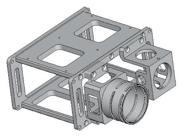
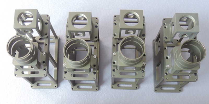
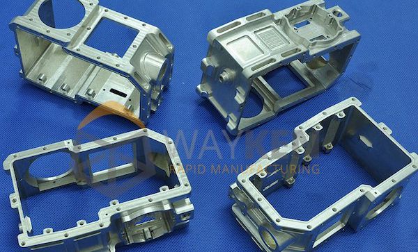
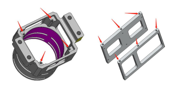
The framework structure shown in the figure consists of 6 parts: Front PCB Support Plate, Back PCB Support Plate, Upper PCB Holder, Bottom PCB Holder, TI Detector Holder, and EO Holder.
- Prevent Deformation When machining PCB Support Plates and Holders
Let’s take a look at the PCB support plates and PCB holders first. As we can see from the picture, the red surfaces are the mounting surface, and the surfaces of the parts are supposed to be aligned with each other, which is then tightened with screws. Therefore, we found a positional tolerance requirement of 0.01 parallelism at the corresponding positions of the drawings for these four parts.
Deformation is the most common problem when machining such thin, flat parts. Because the machining process changes the structural properties of the materials, it also disrupts the stress balance between the material molecules, making it easy for profiles to warp and deform.
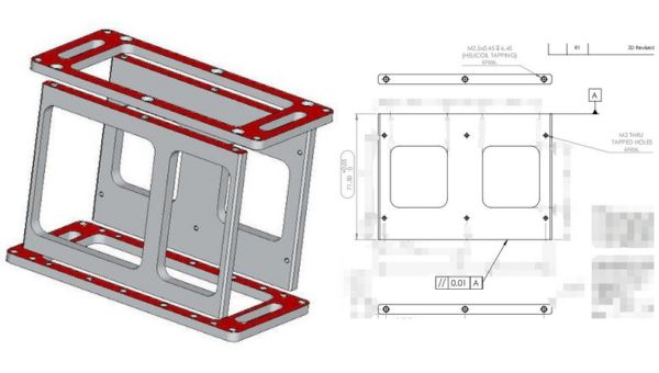
There are typically two ways to overcome this problem:
The first method is to add a heat treatment stabilization process before the final fine machining. This method is usually applied to complex structural parts that require extremely high precision.
The second method is to reduce the feed rate of each maching, and increase machining times. In this way, the stress in the material can be released gradually and slowly. This method is applicable to parts with relatively simple structures.
In this particular case, these four parts can be machined using the logic of the 2nd method, and the precision requirements of the parts can be achieved while controlling the machining costs for the customer.
- Sensor holders
TI Detector Holder and EO Holder are for the sensor parts. The sensor parts detect and collect characteristic signals from the external environment. The deviation of the installation angle and position of sensor components may affect the accuracy of the input data. To ensure the accurate installation of parts, high requirements must be placed on the accuracy of the installation position of the parts.
- The EO holder machining
The EO Holder is the housing of Low Lux CMOS. Accuracy of mounting position is critical for imaging systems. So, we can see from the drawing, the positional accuracy of the purple EO sensor mounting position is defined based on the yellow surface A and the red surface B, and a precision requirement of 0.01mm is proposed. The diameter accuracy of the purple area is +0.02 to +0.05, which not only enables smooth mounting but also effectively limits the vibration of the sensor in the mounting position.
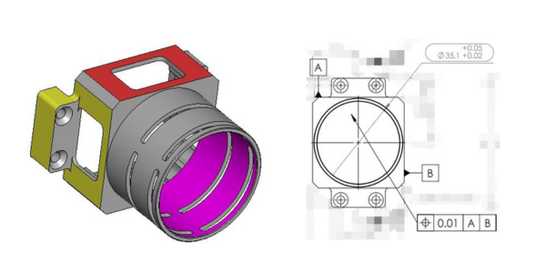
There are three steps when machining the EO holder:
- First, quickly machine the rough appearance of parts, saving time for precision machining in subsequent steps.
- In the second clamping process, the yellow, red and purple surfaces are machined in one pass through the composite turning and milling process, so that these three positional features can meet the requirements of positional accuracy and precision in the drawing.
- Finally, the remaining structural features are machined in the third pass. In this process, it is necessary to design suitable fixtures to prevent deformation of the parts.
- Machining process of TI Detector Holder
TI Detector Holder is the housing for the thermal imager or SWIR imager. From the drawing, we can see that four holes are designed for fixing the key parts in place. In this particular case, the distance between the centers of the circles is very important, we need to maintain a tolerance of ±0.01mm. In order to achieve such precision requirements, we must use appropriate clamping devices to ensure that the workpiece is placed flat and upright.
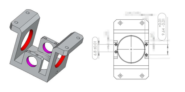
In addition, the two red holes are concentric circles and the two purple holes are concentric circles. Concentric circles should be machined in one pass to ensure concentricity.
3. Considerations for Surface Finishing
Surface treatment is an important step that cannot be ignored after part machining is completed. Ordinary parts are treated with ordinary anodizing for surface treatment. However, for products exposed to extreme environments, military grade III hard anodizing is a better choice.
The oxide layer of three-level hard anodizing is thicker, up to 50 μ above m, the texture is denser and has better resistance to scratching and corrosion.
Aside from the usual operational points to consider in anodizing, there are two other things we need to pay attention to based on the characteristics of the six parts in the case.
- Choose a suitable air pressure for sandblasting
Before the oxidation treatment, we need to sandblast the surface of the parts to cover the knife lines created during CNC machining, so that the surface has a more uniform and perfect texture. Sandblasting is the process of spraying glass beads onto the surface of a part using a high-pressure air stream, covering the original marks on the surface of the part with glass bead pile marks. Excessive impact may cause deformation of the parts, so we should pay attention to adjusting the pressure of the air stream appropriately according to the material, structure and accuracy requirements of the parts.
In our particular case, these 6 parts all deform easily, so we should not set the air pressure too high.
- Carefully remove metal debris from blind holes.
If the metal debris in the blind hole is not thoroughly treated, it will form a compact and hard-to-remove hard block at the bottom of the blind hole after the oxidation treatment, which will affect the effective depth of the blind hole and thread, and affect the assembly of the product.
In our particular case, the Bottom PCB Holder and the Upper PCB Holder each have 6 non-penetrating threads, which are blind hole structures. The EO holder has 4 non-penetrating threads and is a blind hole structure. If it is blocked by metal debris, resulting in insufficient effective thread depth, it will seriously affect the assembly of parts.